Article of scientists of the University of Texas at San Antonio and INAOE in a cover a journal of the Royal Society of Chemistry
The control and manipulation of matter at the nanometric scale to fabricate smart devices capable of storing large amounts of information is a technological challenge. That is what a team of scientists from the University of Texas at San Antonio (UTSA) and the National Institute for Astrophysics, Optics and Electronics (INAOE) have achieved. Scientists at both institutions have fabricated highly ordered three-dimensional nanoarchitectures of magnetic nanowires. This is research that points to hybrid materials with optical and magnetic properties will allow to store large amounts of information in nanometer-sized dimensions.
This work has been published in an article last June and selected as an issue cover art of Material Advances, journal of the Royal Society of Chemistry (RSC) family.
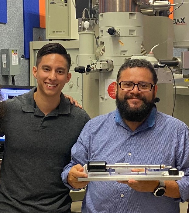
The article entitled "Towards three-dimensional nanoarchitectures: highly ordered bi-layer assembly of tailored magnetic nanowire arrays via template-assisted electrodeposition” under the direction of Dr. Arturo Ponce, from the University of Texas at San Antonio (UTSA) and visiting scientist at INAOE; and participated Arturo Galindo, José Luis Reyes-Rodríguez, and Cristian Botez, also from UTSA, and Dr. Mario Moreno from INAOE. An important part of the work was carried out at INAOE's Microelectronics Lab and the Electron Microscopy laboratory.
Dr. Arturo Ponce, professor and scientist at UTSA and visiting researcher at INAOE, explains that the physical and chemical properties of materials in general, e.g. electronic, optic or magnetic, do not behave the same manner of the material at large scale compared with their counterpart at nanoscale. “The properties of materials at the nanoscale depend on both, the size and the shape in which they have been confined. For instance, a gold nanoparticle or a quantum dot of two nanometers in diameter - to put in context, a nanometer is equal to one billionth of a meter - changes its optical property if the nanoparticle increases its diameter just few nanometers, for example to 5 or 10 nm. Just to cite an example, if the nanoparticle has a pentagonal shape and changes to an elongated form as nano-rod or triangular shape, this will be reflected in a change of its physical properties”, he states.
The researcher adds that in nanotechnology there are two ways to obtain nanomaterials: bottom-up, which consists of building atom-by-atom until the nanostructure is formed, and top-down, which consists of reducing or fragmenting the material on its macroscopic scale down to the nanometer level. The challenge in either way is to control the size and geometric shape in a homogeneous way, he adds.
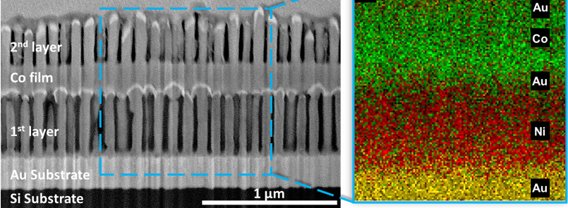
In the work published in the RSC journal, a porous alumina template was used in which nanorods, or nanowires are deposited electrochemically inside the cavities of the template. The nanowires are growing vertically and they are distributed in the area of the alumina template in an orderly manner, forming highly dense bidimensional arrays of nanowires. Templates are prepared by a chemical anodization process of aluminum foils, which oxidizes and, due to the electrochemical potentials of the oxidizing agent, a honeycomb array is formed, that is, a hexagonal arrangement where the cavities will be filled with another electrochemical method to grow the metallic nanowires.
“In this way, we can control the size of the pore diameter, intra-pore distances and lengths and guarantee the same size and thickness of the nanowires. This is an electrochemical method that has been used for several years for various applications. The novelty of our contribution lies in depositing nanowire assemblies by depositing more than one template, which allows us to assemble a nanowire either of the same or another material in order to fabricate three-dimensional nanostructures with hybrid properties, which allows us to have wires in two directions and different materials”.
For this research, transition metals such as cobalt, nickel, gold and silver were used to combine ferromagnetic properties (cobalt and nickel) with plasmonic/optical properties (gold and silver). Optical materials respond to the light that interacts with them, giving rise to collective oscillations of electrons on their surface and having an influence on the magnetic properties of the materials to be assembled. On the other hand, one of the applications of magnetic materials is to store memory. With this arrangement, each wire is intended to be a memory storage site. The highly dense two-dimensional array of many periodically arranged nanowires on the template is aimed at a technology called terabyte per square inch, that is, storing terabytes in one square inch. Our research is aimed at making very small devices with a larger memory capacity, says Dr. Ponce.
“In summary, our interest is to deposit a three-dimensional architecture of self-assemblies at the nanoscale and fabricate materials that have hybrid applications, i.e. optical and magnetic, as well as control memory storage mechanisms through optical stimuli to modulate memory storage through an optical response. That is where our investigations are going, towards making hybrid materials, and control of the phenomenon called magneto-plasmonic coupling”
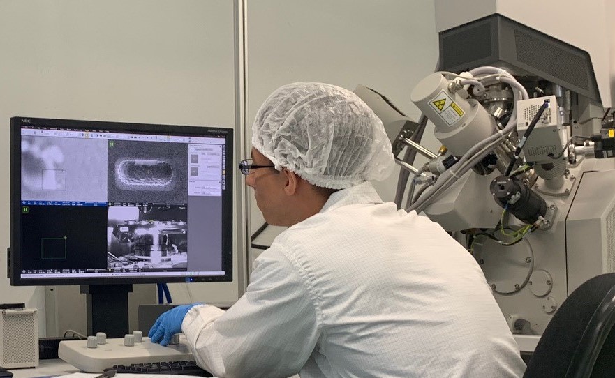
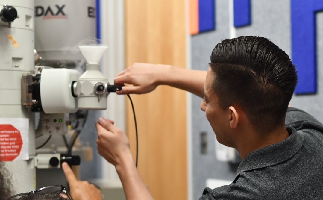
This scientific work was performed at UTSA and INAOE, fabrication and characterization of the nanowires and templates. The analyses the assembly of the multilayers of nanowires were carried out using the dual beam system electron microscope (FIB), electrons-ions, installed in the Laboratory of Electron Microscopy at INAOE. Through nanometric cross-sectional cuts of the multilayers, it was possible to identify the growths of the nanowires, assemblies and characterize them chemically with the chemical detectors coupled to the microscope. Finally, the investigators of this project, Drs. Mario Moreno and Arturo Ponce invite undergraduate and postgraduate students to be part of their research groups for the fabrication of new fascinating structures of intelligent materials confined at the nanoscale.
Luis Enrique Erro # 1, Tonantzintla, Puebla, México, Código Postal 72840, Tel: (222) 266.31.00, difusion@inaoep.mx
This work is licensed under a Creative Commons Attribution-NonCommercial-NoDerivs 2.5 Mexico License.
