INAOE project, recognized as the best of ICANS
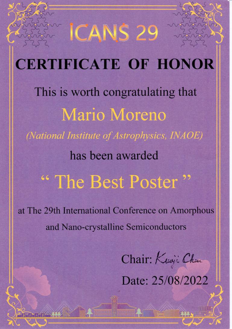
The poster “Deposit, characterization and optimization of microcrystalline germanium thin films”, by doctors Mario Moreno Moreno, Arturo Torres, Alfredo Morales, Alba Arenas, Pedro Rosales, Alfonso Torres, Carlos Zúñiga, Carlos Ascencio, Wilfrido Calleja and Netzahualcoyotl Carlos, from INAOE, and Javier Flores and Roberto Ambrosio, from BUAP, was recognized as the best poster presented at the 29th International Conference on Amorphous and Nano-crystalline Semiconductors, which took place from August 23 to 26 in China.
The International Conference on Amorphous and Nanocrystalline Semiconductors (ICANS) is an excellent space for academic researchers, industry partners and policy makers from around the world to come together and share the latest developments and ideas on the topics of amorphous and nanocrystalline thin film and other materials. of nanostructure.
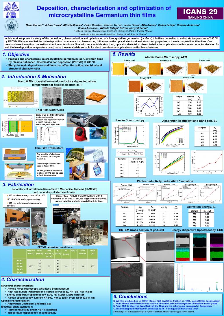
At present, microcrystalline silicon (?c-Si:H) has become an important material for the development and fabrication of large-area semiconductor devices. The method used to deposit these films is by the technique of plasma-assisted chemical vapor deposition (PECVD), at low temperatures using a combination of SiH4 and H2. Currently, thin-film transistors (TFTs) and thin-film solar cells incorporate ?c-Si:H films in their manufacturing processes. However, for some applications it is important to have microcrystalline semiconductors with higher infrared absorption, as in tandem solar cells, and higher carrier mobility, as in TFTs. A less studied material is microcrystalline germanium (?c-Ge:H), which is a complement to ?c-Si:H in some applications.
In the award-winning poster, the authors present a study of the deposition, characterization and optimization of thin films of germanium (?c-Ge:H) deposited at a substrate temperature of 200 °C by PECVD. To do this, they studied the main deposition parameters that have a strong influence on the optical, electrical and structural properties of microcrystalline thin films. The results show the optimal deposition conditions to obtain films with structural, optical and electrical characteristics that are very suitable for applications in thin semiconductor devices. Furthermore, the low deposition temperature used makes these materials suitable for electronic device applications on flexible substrates.
Luis Enrique Erro # 1, Tonantzintla, Puebla, México, Código Postal 72840, Tel: (222) 266.31.00, difusion@inaoep.mx
This work is licensed under a Creative Commons Attribution-NonCommercial-NoDerivs 2.5 Mexico License.
